| CPU Guide |
| Index |
| Intel Processors |
| Overview |
| 486 | Proc [Mhz] |
Voltage [volt] |
Ext Clock [Mhz] |
Pinout | Clock Multiplicator |
Comments |
| SX/DX | 25 | 5 | 25 | 486 | 1 | The DX Version has a FPU |
| SX/DS | 33 | 5 | 33 | 486 | 1 | Math Coprocessor built-in |
| DX | 50 | 5 | 50 | 486 | 1 | |
| DX/2 (SX & DX) |
50 | 5 | 25 | 486 | 2 | The DX Version has a FPU |
| DX/2 (SX & DX) |
66 | 5 | 33 | 486 | 2 | Math Coprocessor built-in |
| DX/4 | 75 | 5 (²) (³) |
25 | 486 | 3 | BOXDX40DPR75 repl 25MHz 486 BOXDX40DP75 if overdrive socket present |
| DX/4 | 100 | 5 (²) (³) |
33 | 486 | 3 | BOXDX40DPR100 repl 33MHz 486 BOXDX40DP100 if overdrive socket present |
| DX/4 | 75 | 3 | 25 | 486 | 3 | A80486DX475 OEM Version |
| DX/4 | 100 | 3 | 33 | 486 | 3 | A80486DX4100 OEM Version |
| Pentium | Proc | Voltage [volt] |
Ext Clock [Mhz] |
Pinout | Clock Multiplicator |
Comments |
| 60 | 5 | 60 | Pent | 1 | ||
| 63 | OD | 5 (³) | 25 | 486 | 2.5 | BOXPODP5V63 repl 25MHz 486 |
| 66 | 5 | 66 | Pent | 1 | ||
| 75 | 3 | 50 | Pent | 1.5 | ||
| 83 | OD | 5 (³) | 33 | 486 | 2.5 | BOXPODP5V83 repl 33MHz 486 Overdrive details |
| 90 | 3 | 60 | Pent | 1.5 | ||
| 100 | 3 | 66 (¹) | Pent | 1.5 | ||
| 120 | 3 | 60 | Pent | 2 | ||
| 120/133 | OD | 5 (³) | 60/66 | Pent | 2 | BOXPODP5V133 repl 60 & 66 MHz |
| 125 | OD | 3 (³) | 50 | Pent | 2.5 | BOXPODP3V125 repl 75 MHz Pentium |
| 133 | 3 | 66 | Pent | 2 | Picture | |
| 150 | 3 | 60 | Pent | 2.5 | ||
| 150 | OD | 3 (³) | 60 | Pent | 2.5 | BOXPODP3V150 repl 90MHz Pentium |
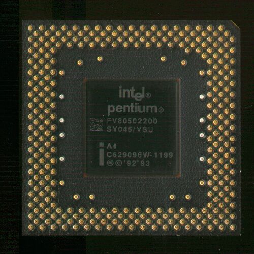
| 166 | 3 | 66 | Pent | 2.5 | Pentium speed comparison | |
| 166 | OD | 3 (³) | 66 | Pent | 2.5 | BOXPODP3V166 repl 100 MHz Pentium |
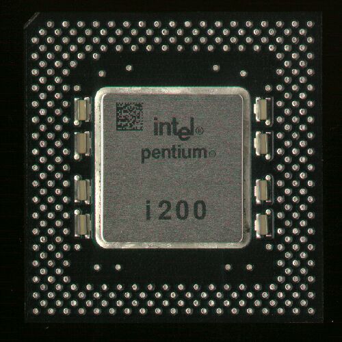
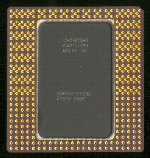
| 200 | 3 | 66 | Pent | 3 | Pentium Technical Data details Picture: top / bottom view |
|
| 233 | 3 | 66 | Pent | 3.5 | Pentium Technical Data details |
| Pentium Pro |
Voltage [volt] |
Ext Clock [Mhz] |
Pinout | Clock Multiplicator |
Comments |
| 150 | 3 | 60 | PPro | 2.5 | Details on Pentium Pro |
| 166 | 3 | 66 | PPro | 2.5 | |
| 180 | 3 | 60 | PPro | 3 | |
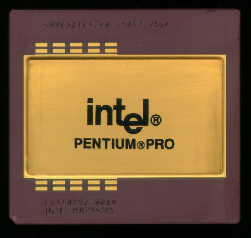
| 200 | 3 | 66 | PPro | 3 | Picture: top / bottom view |
| (¹) | Some motherboards connect a special pin to ground, forcing the processor to run on 50MHz externally |
| (²) | The processor-core runs on 3.3V, however, the Voltageregulator on top of the chip converts the 5V supply to 3.3V |
| (³) | This chip has a builtin heat sink |
| Note: The
PCI Bus Clock is always half of the external CPU Clock speed (e.g. a P166 will have a PCI
Bus Clock of 33 MHz) EISA & ISA Systems have at most a 8MHz Bus Clock (4.77MHz
minimum). All Overdrive (OD) Processors are direct chip replacements
and require no modifiaction of the switch or jumper settings on the motherboard. |
| Index |
| Quality and other marks on the Intel Pentium Processors |
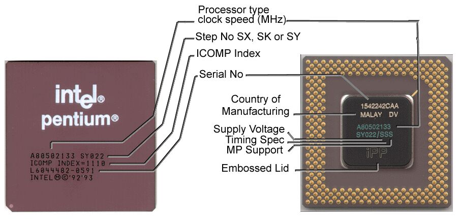 |
| Mark | Example | What it stands for |
| Processor type | A80502133 | Where A80502 stands for Pentium Processor and 133 for the max. Clockspeed (i.e. 133 MHz) It could also be something like -75 which would be a 75 MHz CPU |
| Step No | SX022/SSS SK022/SSS SY022/SSS |
Where SY022 stands for what lithography mask Intel used to make this particular processor and SSS see below |
| Supply Voltage | S V |
S stands for Standard 3.135V to 3.6V V stands for VRE with operating voltages narrowed it to 3.4V to 3.6V, this 'V' Version might not be compatible w/ the Powersupply in your PC Timing Spec |
| Timing Spec | S M |
S stands for Standard M stands for Min Valid Delay Specification, this 'M' Version requires very strict timing from your system |
| MP Support | S U |
S stands for Standard where you can use the
CPU in any Dual, Multi or single CPU configuration U stands for Uniprocessor only, this version can not be used in a system with more than one CPU, and is typically suited for Desktop PC's |
| Embossed Lid | iPP | iPP is the mark all 90MHz and faster CPU's
carry. Most 75MHz Pentiums carry only the i75 symbol. |
| ICOMP Index | 1110 | This is the standard Intel CPU Speed Index |
| Serial No | L6044482 | The Serial No consists of the actual number and -0591 the serialcode, together they form a unique number |
| Country of manufacture | MALAY | The CPU shown was manufactured in Intels Malaysia facility. Some people consider the CPU's made in the Philippines better, however, there is no real reason for this judgement Intel does not mark all CPU's w/ the country of origin |
| * These marks are not on all CPU's
manufactured by Intel. Generally speaking a CPU made
in the Philippines w/ a SSS mark after the Step No is considered the best quality
obtainable from Intel, however Intels practices make it virtually impossible to predict
what grade of CPU's you receive, when the order is placed w/ Intel.
|
| Index |
| Intel CPU Markings FAQ |
Question:
Answer:
|
Question:
Answer:
Here is the decoding of ABC:
|
Question:
Answer:
NOTES:
|
Question:
Answer:
|
| Index |